AI 반도체의 새로운 토대, 유리기판이란 무엇인가?: 기초부터 핵심 원리까지
「유리기판 완전정복」 연재 · 1번째 글
이 글은 「유리기판 완전정복」 연재의 출발점입니다.
최근 반도체 시장의 가장 뜨거운 화두 중 하나는 단연 ‘유리기판(Glass Substrate)’입니다. 인공지능(AI) 기술이 폭발적으로 발전하면서, 이를 구동하는 반도체 칩은 점점 더 크고 강력해지고 있습니다. 하지만 칩을 받쳐주는 ‘토대’가 그 무게와 열을 감당하지 못하는 문제가 발생하기 시작했습니다.
이 글에서는 반도체 기술의 패러다임을 바꿀 게임 체인저로 불리는 유리기판이 정확히 무엇인지, 왜 지금 모든 빅테크 기업들이 이 기술에 주목하는지, 그리고 어떤 원리로 작동하는지 차근차근 해설해 드리고자 합니다. 이 글은 특정 종목의 투자를 추천하는 것이 아닌, 기술의 근본적인 개념과 구조를 이해하여 독자 여러분이 스스로 판단의 근거를 마련하는 데 도움을 드리는 ‘토대 해설 글’입니다.
유리기판이란 무엇인가? (정의)
가장 먼저, 유리기판이 무엇인지 그 정체부터 명확히 짚고 넘어가겠습니다. 우리가 사는 초고층 빌딩이 흔들림 없이 서 있으려면 땅속 깊이 박힌 단단한 암반 위에 지어야 하는 것과 같습니다. 만약 무른 땅 위에 빌딩을 올리면 어떻게 될까요? 건물 무게를 이기지 못하고 기울거나 내려앉아 큰 사고로 이어질 것입니다.
반도체 칩도 마찬가지입니다. 여기서 수많은 전자회로가 새겨진 반도체 칩(Die)이 ‘초고층 빌딩’이라면, 이 칩을 밑에서 받쳐주고 메인보드와 전기적으로 연결해주는 얇은 판이 바로 ‘기판(Substrate)’입니다. 기판은 칩에 전원을 공급하고 신호를 전달하는 동시에, 칩을 외부 충격으로부터 보호하는 ‘건물의 기초’와 같은 역할을 합니다.
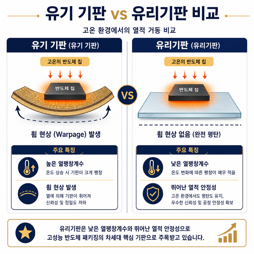
지금까지는 이 기판을 주로 플라스틱 수지(ABF, Ajinomoto Build-up Film 등)로 만들어 왔습니다 [1]. 하지만 AI 반도체처럼 고성능 칩은 작동 시 엄청난 열을 발생시키는데, 플라스틱 기반의 유기 기판은 이 열을 견디지 못하고 감자칩처럼 휘어지는 ‘휨 현상(Warpage)’이라는 심각한 문제에 직면했습니다 [1][42]. 이 휨 현상은 기판과 칩을 연결하는 수만 개의 미세한 연결 부위에 균열을 일으켜 반도체 전체를 망가뜨리는 치명적인 불량의 원인이 됩니다 [42].
유리기판은 바로 이 문제를 해결하기 위해 등장한 대안입니다. 이름 그대로, 기존의 플라스틱 소재 대신 구조적으로 훨씬 단단하고 열에 의한 변형이 거의 없는 특수 유리를 사용해 만든 차세대 반도체 기판입니다 [1]. 플라스틱이라는 무른 땅 대신, 유리라는 단단한 암반으로 기초 공사를 다시 하는 것에 비유할 수 있습니다.
한 줄 정리: 유리기판은 AI 반도체의 성능을 감당하지 못하는 기존 플라스틱 기판을 대체하기 위해 등장한, 유리로 만든 단단하고 열에 강한 ‘첨단 반도체용 인쇄회로기판’입니다.
유리기판은 어떻게 작동하는가? (작동 원리)
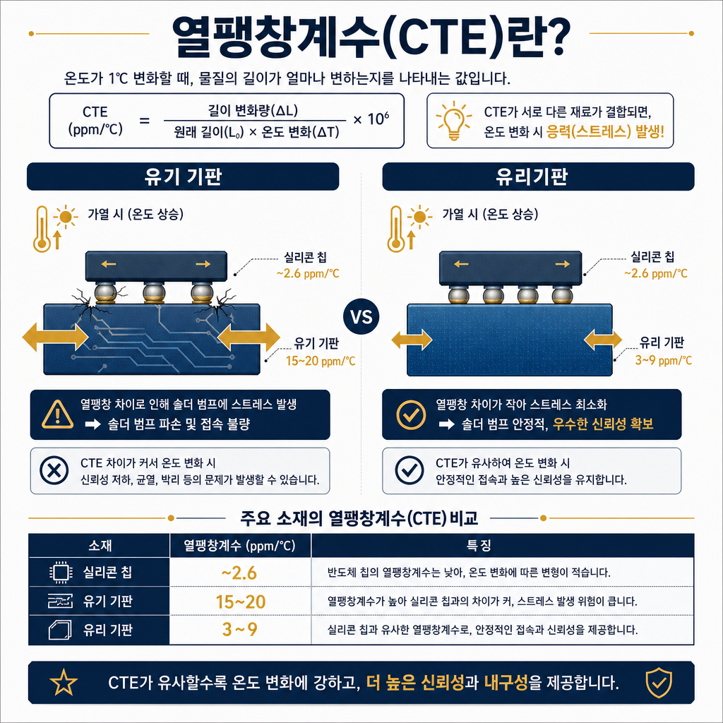
그렇다면 유리는 어떻게 플라스틱이 해결하지 못한 문제를 해결할 수 있었을까요? 그 비밀은 ‘열팽창계수(CTE, Coefficient of Thermal Expansion)’라는 개념에 있습니다. 조금 어려운 용어 같지만, 뜨거운 프라이팬에 갑자기 찬물을 부었을 때 ‘치익’ 소리를 내며 뒤틀리는 현상을 떠올리면 쉽습니다. 이는 서로 다른 온도의 물질이 만나 급격히 수축하고 팽창하면서 발생하는 스트레스 때문입니다.
반도체 패키지 내부에서도 비슷한 일이 일어납니다. 반도체 칩은 주로 실리콘으로 만들어지는데, 이 실리콘은 열을 받아도 팽창하는 정도가 매우 낮습니다 [3]. 그에 반해 기존의 플라스틱 기판은 열을 받으면 실리콘보다 훨씬 많이 팽창합니다 [3]. 즉, ‘칩’이라는 프라이팬과 ‘기판’이라는 가스레인지가 서로 다른 속도로 늘어났다 줄어들다 보니, 그 둘을 붙잡고 있는 수만 개의 연결 단자들이 스트레스를 이기지 못하고 끊어지는 것입니다.
유리기판의 핵심 작동 원리는 바로 이 열팽창계수를 반도체 칩의 소재인 실리콘과 거의 비슷하게 ‘맞춰주는(Tuning)’ 것입니다 [1][3]. 특수하게 조성된 유리는 열팽창계수(CTE)를 실리콘(약 2.6 ppm/°C)과 매우 유사한 3~9 ppm/°C 수준으로 정밀하게 조절할 수 있습니다 [3]. 이는 15~20 ppm/°C에 달하는 기존 유기 기판과는 비교할 수 없는 수준입니다 [3].
이렇게 칩과 기판의 열팽창률이 비슷해지면, 1,000와트(W)가 넘는 전력을 소모하는 AI 가속기가 뜨겁게 달아올라도 칩과 기판이 한 몸처럼 움직이게 됩니다 [3]. 덕분에 연결 부위에 가해지는 스트레스가 50% 이상 감소하고, 제품의 신뢰성과 수명을 획기적으로 높일 수 있습니다 [3].
여기에 더해, 유리는 원자 단위 수준의 완벽한 평탄도를 자랑합니다 [1-3]. 이는 마치 구겨진 종이가 아닌 빳빳하고 매끄러운 고급 용지 위에 더 정밀한 그림을 그릴 수 있는 것과 같습니다. 기판이 평평할수록 더 미세하고 촘촘한 회로를 새겨 넣을 수 있어, AI 반도체가 요구하는 초고밀도 회로 구현에 절대적으로 유리합니다 [2].
한 줄 정리: 유리기판은 반도체 칩과 거의 동일한 비율로 열에 팽창하고 수축하도록 ‘열팽창계수(CTE)’를 조절해, 열로 인한 변형과 신호 왜곡을 최소화하는 원리로 작동합니다.
유리기판은 무엇으로 만들어지는가? (구조 분해)
유리기판은 단순히 창문 유리를 잘라 만드는 것이 아닙니다. 반도체의 혹독한 환경을 견디기 위해 특별히 설계된 첨단 소재와 구조로 이루어져 있습니다. 크게 ‘소재’와 ‘구조’ 두 가지로 나누어 살펴보겠습니다.
핵심 소재: 특수 목적용 첨단 유리
마치 요리사가 용도에 따라 다른 종류의 밀가루를 쓰듯, 유리기판 제조사들도 저마다의 특화된 유리 소재를 개발해 경쟁하고 있습니다. 현재 시장을 주도하는 대표적인 기업과 소재는 다음과 같습니다.
- 코닝 (Corning, 미국): 디스플레이 유리 시장의 강자인 코닝은 독자적인 ‘퓨전(Fusion) 공법’을 통해 별도의 연마 과정 없이도 표면이 극도로 매끄러운(1.0nm 미만) 유리를 생산합니다 [4][6]. 고객사 요구에 맞춰 다양한 열팽창계수 라인업을 제공하며, 대면적 패널 생산에 강점을 보입니다 [4][25].
- 쇼트 (Schott, 독일): 100년 이상의 역사를 가진 특수유리 명가 쇼트는 붕규산, 알루미노규산계 등 매우 폭넓은 소재 포트폴리오를 자랑합니다 [26]. 대표 제품인 ‘AF 32 eco’는 실리콘과 열팽창계수가 유사하며, 머리카락보다 얇은 12µm(마이크로미터) 초박막 유리까지 생산할 수 있는 기술력을 갖추고 있습니다 [10][11].
- AGC (일본): 실리콘과 CTE가 매우 유사한(3.8 ppm/°C) 무알칼리 유리 ‘EN-A1’을 주력으로 내세우고 있습니다 [15][16]. 특히 정밀한 레이저 가공 기술과 결합해 유리기판의 핵심 구조인 ‘TGV’ 구현에 특화된 솔루션을 제공합니다 [19][20].
- NEG (Nippon Electric Glass, 일본): 일반 유리보다 가공성과 기계적 강도를 높인 특수 유리 세라믹 소재 ‘GC Core’를 개발해 차별화를 꾀하고 있습니다 [27][28]. CO2 레이저를 이용한 고속 가공에 유리한 특징을 가집니다 [27].
핵심 구조: 전기 신호의 엘리베이터, TGV
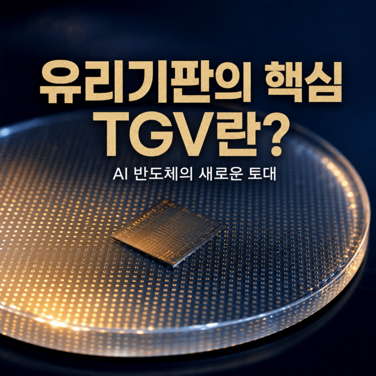
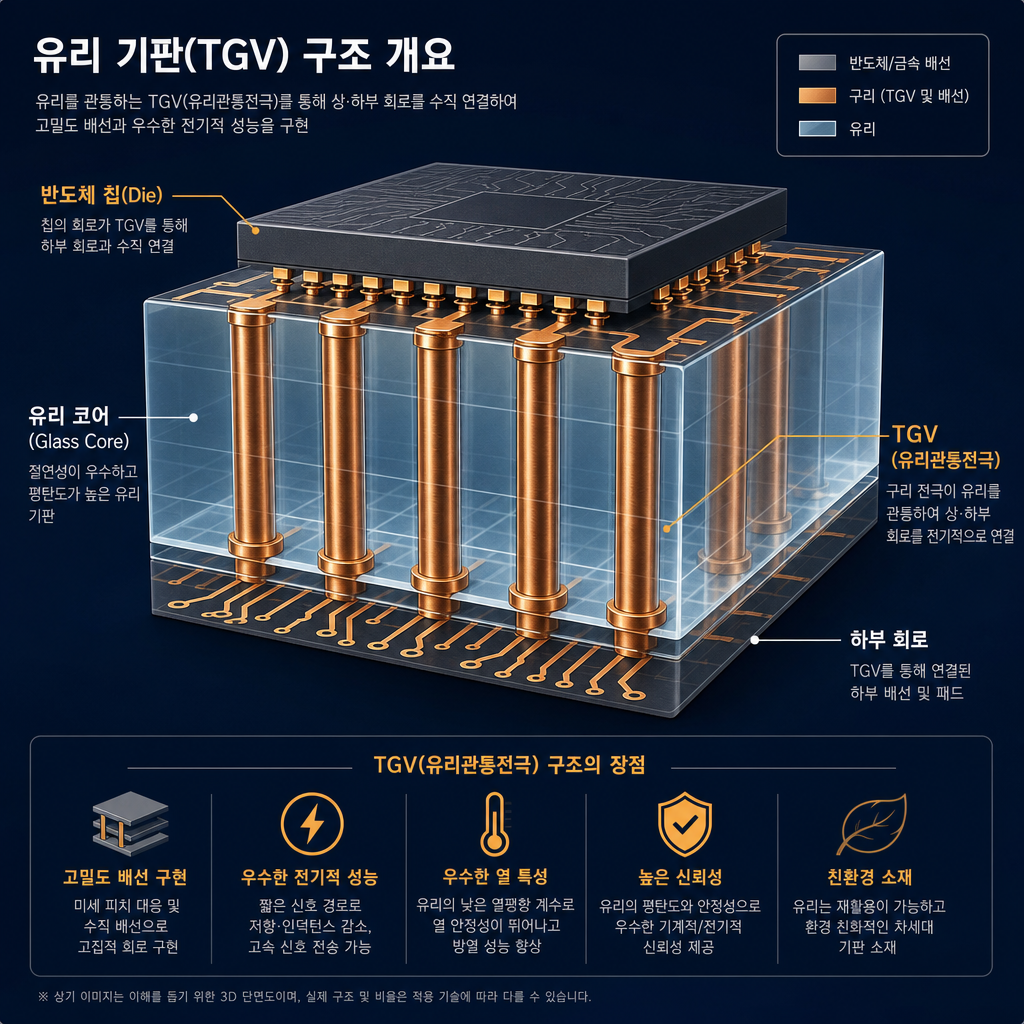
유리는 전기가 통하지 않는 절연체입니다. 따라서 기판의 위층과 아래층, 그리고 반도체 칩과 메인보드를 연결하려면 전기 신호가 지나다닐 수 있는 ‘통로’를 만들어 주어야 합니다. 이 통로가 바로 ‘TGV(Through-Glass Via, 유리관통전극)’입니다.
TGV는 눈에 보이지 않을 정도로 미세한 구멍을 유리에 수직으로 뚫고, 그 안을 구리(Cu)와 같은 전도성 물질로 채워 넣은 것입니다. 이는 마치 여러 층으로 이루어진 건물에서 각 층을 연결하는 ‘엘리베이터’와 같습니다. 수십만 개의 TGV가 유리기판 내부에서 전기 신호를 빠르고 정확하게 전달하는 역할을 수행합니다. 이 TGV를 얼마나 작고 촘촘하게, 그리고 균일하게 만드느냐가 유리기판 기술의 핵심 경쟁력이라 할 수 있습니다.
한 줄 정리: 유리기판은 코닝, 쇼트 등이 만드는 특수 조성 유리(붕규산, 알루미노규산계 등)를 핵심 재료로 하며, 유리 내부를 관통하는 미세한 구리 전극 ‘TGV’를 통해 전기 신호를 전달하는 구조를 가집니다.
유리기판의 장점과 아직 남은 과제는?
모든 신기술이 그렇듯, 유리기판 역시 엄청난 잠재력과 함께 아직 넘어야 할 기술적 과제를 동시에 안고 있습니다. 마치 F1 경주용 자동차가 폭발적인 성능을 내지만, 그만큼 다루기 까다롭고 비싼 것과 같습니다.
명확한 장점: 성능과 효율의 두 마리 토끼
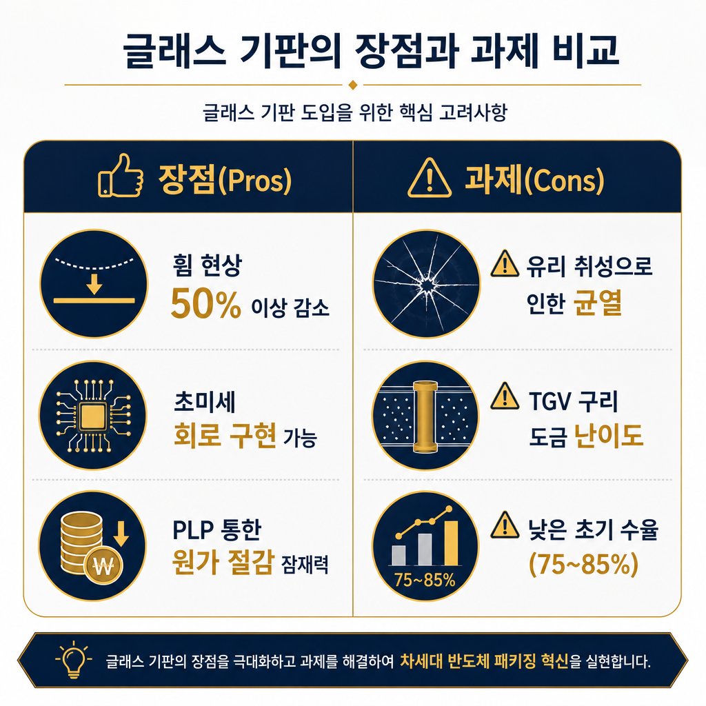
- 압도적인 구조적 안정성: 유리기판은 기존 유기 기판 대비 휨 현상을 50% 이상 줄일 수 있습니다 [38]. 이는 대형 AI 칩을 안정적으로 지지하며, 수율(생산품 대비 양품 비율)을 높이는 데 결정적인 역할을 합니다 [42].
- 초미세 회로 구현: 매끄러운 표면 덕분에 2µm 이하의 초미세 회로 패턴을 그릴 수 있어, 더 많은 데이터를 더 빠르게 처리해야 하는 AI 반도체의 요구를 충족시킬 수 있습니다 [2].
- 원가 절감 잠재력(PLP): 유리기판은 처음부터 ‘패널레벨 패키징(PLP, Panel-Level Packaging)’을 염두에 두고 개발되었습니다. 이는 빵을 구울 때 작은 원형 틀 대신 커다란 사각 오븐 트레이를 사용해 한 번에 훨씬 많은 양을 굽는 것과 같은 원리입니다. 기존의 300mm 둥근 웨이퍼 대신 515mm x 510mm 크기의 대형 사각 패널을 사용하면, 한 번에 처리하는 면적이 3.7배나 넓어집니다 [100]. 이를 통해 패키징 비용을 30~40%까지 획기적으로 절감할 수 있는 잠재력을 가집니다 [96][101].
극복해야 할 과제: ‘깨짐’과 ‘채움’의 문제
- 근본적인 취성(Brittleness): 유리의 가장 큰 약점은 ‘깨지기 쉽다’는 것입니다. TGV 공정을 위해 유리에 구멍을 뚫을 때, 눈에 보이지 않는 5~20μm 크기의 미세 균열(Micro-crack)이 발생할 수 있습니다 [29][31]. 이 작은 균열이 후속 공정에서 거대한 파손으로 이어져 수율을 떨어뜨리는 주범이 됩니다 [32-36]. 특히 공정이 끝난 기판을 최종 제품 크기로 자를 때 유리가 상하로 쪼개지는 ‘사와레(SeWaRe)’ 불량은 업계의 가장 큰 난제 중 하나입니다 [35].
- TGV 도금의 어려움: 직경 100μm, 깊이 800μm에 달하는 좁고 깊은 구멍 수십만 개를 빈틈(Void) 없이 완벽하게 구리로 채우는 것은 매우 정교한 기술을 요구합니다 [37]. 만약 미세한 기포라도 발생하면 전기적 불량의 원인이 될 수 있습니다 [38]. 또한, 구리와 유리의 열팽창계수 차이 때문에 장기적으로 구리가 유리에서 떨어져 나가는 ‘박리(Delamination)’ 현상이 발생할 위험도 있습니다 [39-41].
- 낮은 수율과 높은 초기 비용: 이러한 공정 난이도 때문에, 현재 유리기판의 수율은 75~85% 수준으로, 90~95%에 달하는 성숙한 유기 기판에 비해 아직 낮습니다 [45][82]. 이는 단위 면적당 제조 원가가 기존 기판 대비 2~3배가량 높아지는 직접적인 원인이 됩니다 [81].
한 줄 정리: 휨 현상 감소와 대면적 생산 잠재력이란 큰 장점이 있지만, 유리의 깨지기 쉬운 특성(취성)과 TGV 공정의 어려움으로 인한 낮은 수율과 높은 초기 비용이 해결해야 할 과제입니다.
어떤 기업들이 유리기판을 사용하나? (산업 적용)
유리기판은 더 이상 실험실 안의 기술이 아닙니다. 반도체 산업의 지형을 바꿀 거대한 흐름으로, 글로벌 빅테크 기업들이 시장 선점을 위해 치열한 속도 경쟁을 벌이고 있습니다.
2026년, 상용화 원년의 서막
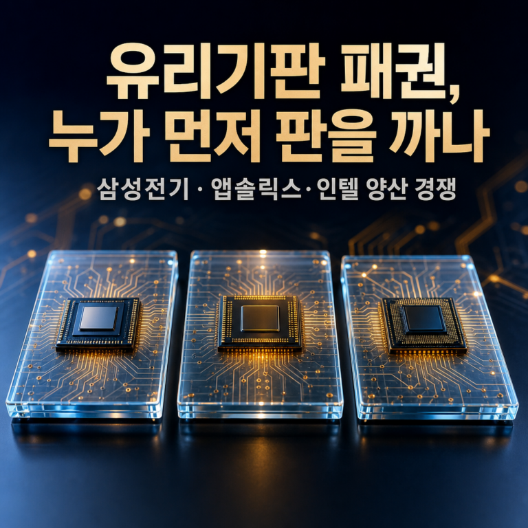
현재 시점(2026년 6월)은 유리기판 상용화의 원년이라 할 수 있습니다. 인텔(Intel)이 이 경쟁의 선두 주자로, 2026년 초 데이터센터용 프로세서 ‘제온 6+(Xeon 6+)’에 세계 최초로 유리기판 기술을 적용해 대량 양산을 시작했습니다 [57][59]. 이는 유리기판이 실제 상업용 제품에 탑재된 역사적인 첫 사례입니다.
AI 칩의 절대강자인 엔비디아(NVIDIA) 역시 올해 하반기 출시할 ‘GB200’ 칩의 첨단 패키징에 유리기판 도입을 계획하고 있으며 [60], 경쟁사인 AMD도 SKC의 자회사 앱솔릭스 등과 함께 차세대 AI 가속기용 유리기판 프로토타입의 성능 평가를 진행 중입니다 [61][63]. 파운드리 1위 기업인 TSMC도 2026년 파일럿 라인 구축을 목표로 기술 개발에 박차를 가하고 있습니다 [64].
2027년~2030년, 본격적인 개화기
업계에서는 2027년을 유리기판이 본격적으로 상업화되는 시점으로 보고 있으며, 엔비디아와 구글(Google)이 초기 시장을 이끌 핵심 고객사가 될 것으로 전망합니다 [65][67]. 후공정(OSAT) 1위 기업인 대만의 ASE는 2027년 상반기부터 패널레벨 패키징 자동화 라인을 가동할 예정입니다 [68].
이후 2028년에는 기술 채택이 더욱 가속화될 전망입니다. 엔비디아는 차세대 ‘파인만(Feynman)’ 아키텍처 GPU에 유리기판 기술을 전면 도입하고 [69][70], AMD는 기존에 사용하던 실리콘 인터포저를 유리 인터포저로 완전히 대체할 계획입니다 [71][72]. TSMC와 앰코(Amkor) 같은 주요 파운드리 및 후공정 업체들도 2028년부터 대규모 양산을 시작하며 생태계는 더욱 확장될 것입니다 [73][75].
궁극적으로 인텔은 2030년까지 광신호를 이용하는 차세대 기술(CPO)까지 유리기판에 통합하여, 단일 칩 패키지에 1조 개의 트랜지스터를 집적한다는 원대한 목표를 향해 나아가고 있습니다 [76-80]. 이러한 흐름은 미국 정부가 칩스법(CHIPS Act)을 통해 SKC의 자회사 앱솔릭스(Absolics)에 7,500만 달러의 생산 보조금과 1억 달러의 R&D 보조금을 지원하는 등 [108][113], 각국 정부가 미래 반도체 패권이 걸린 전략 기술로 인식하고 국가적 지원에 나서는 배경이 되고 있습니다.
한 줄 정리: 인텔이 2026년 세계 최초 상용화를 시작으로, 엔비디아, AMD, TSMC 등 거의 모든 반도체 대기업이 2027-2030년을 목표로 유리기판 도입 로드맵을 발표하며 치열하게 경쟁하고 있습니다.

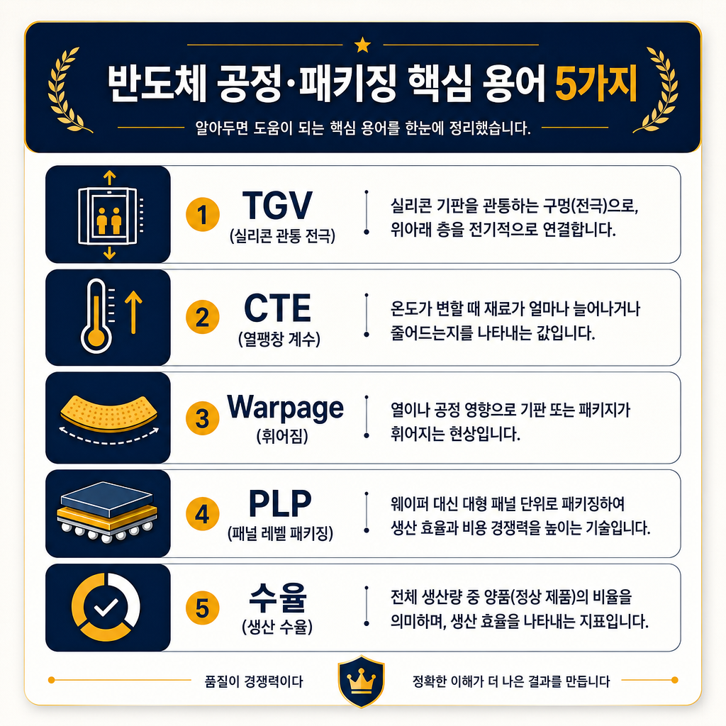
꼭 알아야 할 핵심 용어 정리
이 글을 통해 유리기판의 세계를 처음 접하신 분들을 위해, 반드시 기억해야 할 5가지 핵심 용어를 마지막으로 정리해 드립니다. 이 용어들만 알아도 앞으로 관련 뉴스를 이해하는 데 큰 도움이 될 것입니다.
- TGV (Through-Glass Via, 유리관통전극): 유리기판의 위아래 층을 전기적으로 연결하기 위해 유리를 수직으로 관통하는 미세한 구리 기둥을 말합니다. 칩 내부의 ‘엘리베이터’와 같은 핵심적인 역할을 합니다.
- CTE (Coefficient of Thermal Expansion, 열팽창계수): 온도가 변할 때 물질이 팽창하거나 수축하는 정도를 나타내는 값입니다. 반도체 칩과 기판의 CTE 수치가 비슷해야 열로 인한 뒤틀림이나 파손을 막을 수 있습니다.
- Warpage (휨 현상): 주로 열 때문에 기판이 평평함을 잃고 감자칩처럼 휘어지는 현상입니다. 이는 반도체 불량의 주된 원인 중 하나로, 유리기판이 해결하고자 하는 가장 중요한 문제입니다.
- PLP (Panel-Level Packaging, 패널레벨 패키징): 기존의 작고 둥근 웨이퍼 대신, 크고 네모난 패널 위에서 한 번에 많은 칩을 패키징하여 생산 효율을 극대화하는 방식입니다. 유리기판의 원가 경쟁력을 확보하기 위한 핵심 전략입니다.
- 수율 (Yield): 전체 생산품 중에서 정상적으로 작동하는 양품의 비율을 의미합니다. 수율이 높을수록 생산성이 좋고 원가가 낮아지기 때문에 반도체 제조에서 가장 중요한 지표 중 하나입니다.
지금까지 AI 시대의 새로운 반도체 토대, 유리기판에 대해 알아보았습니다. 아직은 높은 비용과 기술적 난제라는 장벽이 존재하지만, AI 반도체의 성능 한계를 돌파하기 위한 유일한 대안으로 지목되는 만큼, 앞으로 반도체 산업의 지형을 바꿀 가장 중요한 기술이 될 것임은 분명해 보입니다.
한 줄 정리: TGV(수직 전극), CTE(열팽창계수), Warpage(휨 현상), PLP(대면적 생산), 수율(양품 비율)은 유리기판 기술을 이해하는 데 가장 중요한 5가지 핵심 키워드입니다.
References
▶ research4lab.tistory.com · 차세대 반도체 패키징의 패러다임 전환: 인텔(Intel)의 유리기판(Glass Substrate) 기술 혁신과 미래 시장 전망
https://research4lab.tistory.com/entry/%EC%B0%A8%EC%84%B8%EB%8C%80-%EB%B0%98%EB%8F%84%EC%B2%B4-%ED%8C%A8%ED%82%A4%EC%A7%95%EC%9D%98-%ED%8C%A8%EB%9F%AC%EB%8B%A4%EC%9E%84-%EC%A0%84%ED%99%98-%EC%9D%B8%ED%85%94Intel%EC%9D%98-%EC%9C%A0%EB%A6%AC%EA%B8%B0%ED%8C%90Glass-Substrate-%EA%B8%B0%EC%88%A0-%ED%98%81%EC%8B%A0%EA%B3%BC-%EB%AF%B8%EB%9E%98-%EC%8B%9C%EC%9E%A5-%EC%A0%84%EB%A7%9D
- [1] “그러나 기존에 널리 사용되던 아지노모토 빌드업 필름(ABF, Ajinomoto Build-up Film)과 구리 적층판(CCL, Copper…”
- [3] “둘째, 열역학적 관점에서 유리는 실리콘 다이(Die)와의 열팽창계수(CTE) 불일치를 해결할 수 있는 튜닝(Tuning) 가능성을 지니고…”
- [42] “그러나 기존에 널리 사용되던 아지노모토 빌드업 필름(ABF, Ajinomoto Build-up Film)과 구리 적층판(CCL, Copper…”
- [64] “앱솔릭스 또한 인텔 및 SK하이닉스 출신의 반도체 패키징 전문가인 강지호 부사장을 신임 CEO(김종우 전임 CEO 교체)로 임명하여…”
- [96] “패널 단위 노광 장비(예: Onto Innovation, Canon의 장비)의 발전과 렌즈 개구수(Numerical Aperture)…”
- [100] “경제성 확보: 패널 레벨 패키징(FOPLP) 로드맵과 비용 절감 전망 2026년 3월 현재 기술의 완성도는 입증되었으나, 경제성 측면에서…”
- [125] “이러한 지속가능성 행보는 시장 선발 주자인 인텔의 행보와도 궤를 같이한다. 인텔은 유리기판 선행 연구 및 대량 양산의 전초기지인 미국…”
▶ Chip Scale Review · Chip Scale Review • Spring • 2026
https://chipscalereview.com/wp-content/uploads/2026/04/Chip-Scale-Review-Spring-2026-digital.pdf
- [2] “Glass provides a sophisticated solution to this thermo-mechanical crisis. Its…”
▶ Corning · Carrier Solutions Standard Glass Carriers
https://www.corning.com/media/worldwide/csm/documents/Carrier%20Solutions%20Standard%20Glass%20Carrier.pdf
- [4] “Options and Features CTE Offerings 3.4 x10⁻⁶/ºC – 10×10-6/ºC Form Factors…”
- [25] “process environments Carrier Solutions Standard Glass Carriers Carrier…”
▶ Corning · Development of Substrates Featuring Through Glass Vias (TGV) for 3D-IC Integration
https://www.corning.com/media/worldwide/global/documents/semi%20Development%20of%20Substrates%20Featuring%20TGV%20and%203D-IC%20Integration.pdf
- [6] “Corning Fusion Glass Unpolished Ra = 1.7 Å Polished Glass Ra = 6.0 Å…”
- [7] “Introduction There are two primary challenges to fabricating a precision…”
▶ Schott · Electrical Properties of SCHOTT Thin Glasses
https://www.schott.com/en-dk/products/d-263/-/media/project/onex/products/d/d263/downloads/row-schott-electrical-properties-datenflyer-view-2019-05-24_.pdf
- [13] “ρD at ϑ = 250 °C in Ω·cm 1.18 ·108 ρD at ϑ = 350 °C in Ω·cm 4.24 ·106 SCHOTT…”
▶ pgo-online.com · AF 32® eco | Alkali-free glass for semiconductor & MEMS
https://www.pgo-online.com/intl/af32.html
- [10] “Special Properties Alkali-free in synthesis* Low thermal expansion coefficient…”
- [11] “Available in 48-hour express service AF 32 ® eco is an advanced flat…”
▶ MDPI · Application of Through Glass Via (TGV) Technology for Sensors Manufacturing and Packaging
https://www.mdpi.com/1424-8220/24/1/171
- [12] “2. Through Glass Vias’ Formation and Metallization Techniques Glasses,…”
▶ Abrisa … · AGC EN-A1 Alkali Free Boro-Aluminosilicate Glass
https://abrisatechnologies.com/media/AGC-EN-A1.pdf
- [15] “Thermal Properties CTE (Thermal Expansion) (50-250ºC) x 10 -7 / ºC 38 Glass…”
▶ note.com · Implementation Infrastructure for Photoelectric Fusion Supporting …
https://note.com/rosy_takin7329/n/n679d93086232?hl=en
- [16] “Physical and Electrical Advantages Provided by Glass Substrates The reason why…”
- [19] “Precision Drilling Technology and Aspect Ratio AGC’s TGV technology makes it…”
- [45] “● Instability of yield : Due to cracks during processing caused by the…”
- [81] “Economic Challenges and Ensuring Scalability Regarding the commercialization…”
- [90] “● Instability of yield : Due to cracks during processing caused by the…”
▶ AGC · AGC’s Semiconductor Solutions Pioneering the Future of AI – CES 2026
https://www.agc.com/en/ces/semiconductor.html
- [18] “Glass Core / Interposer TGV Glass Substrate for Advanced Packaging AGC can…”
▶ AGC ELECTRONICS TAIWAN INC · Through Glass Via
https://www.agc-electronics.com.tw/eng/semiconductor/59376483.html
- [20] “High speed It enables high speed and large capacity communication with…”
▶ Nippon Electric Glass (NEG) · NEG’s Glass Substrates for Next-Generation Semiconductors
https://www.neg.co.jp/en/neg-journal/20260201.html
- [22] “Thinner design and improved handling due to high strength • Specifications can…”
- [27] “Features of NEG’s Glass Substrates To overcome the challenges of glass…”
- [28] “관련주정리 – 유리 소재: 코닝, Schott, NEG 기업 국가 사업영역 기존사업및글라스 기판시장진출현황 코닝 미국 유리 소재 – 애플의…”
▶ 할로파파 · 차세대 반도체 패키징용 유리기판 소재 공정기술 동향
https://hollopapa.tistory.com/entry/%EC%B0%A8%EC%84%B8%EB%8C%80-%EB%B0%98%EB%8F%84%EC%B2%B4-%ED%8C%A8%ED%82%A4%EC%A7%95%EC%9A%A9-%EC%9C%A0%EB%A6%AC%EA%B8%B0%ED%8C%90-%EC%86%8C%EC%9E%AC-%EA%B3%B5%EC%A0%95%EA%B8%B0%EC%88%A0-%EB%8F%99%ED%96%A5
- [26] “유리기판 소재 공정기술의 개요 기술의 개념 유리기판 소재 공정기술은 고성능 메모리·GPU·CPU 반도체 패키지에 필요한 대면적 구현이…”
▶ PatSnap Eureka · Glass Core Substrate Material: Advanced Architectures And …
https://eureka.patsnap.com/materials/glass-core-substrate-material
- [29] “Through-glass via (TGV) formation represents the most technically challenging…”
- [30] “Through-glass via (TGV) formation represents the most technically challenging…”
▶ PatSnap Eureka · Glass Substrate For Semiconductor Packaging: Advanced Materials Engineering And Integration Strategies
https://eureka.patsnap.com/materials/glass-substrate-semiconductor
- [31] “TGV Formation: Laser Drilling And Etching Techniques Through-glass via…”
- [43] “Stress Distribution And Warpage Control Stress management is critical in…”
- [44] “The stress measurement is performed by photoelastic analysis or X-ray…”
▶ MDPI · A Review of Glass Substrate Technologies
https://www.mdpi.com/2674-0729/4/3/37
- [32] “After TGV copper filling, subsequent processing steps can induce stress within…”
- [33] “After TGV copper filling, subsequent processing steps can induce stress within…”
- [34] “After TGV copper filling, subsequent processing steps can induce stress within…”
▶ 디일렉 · [Y인사이트] 유리기판으로 반도체 패키징 혁신! 중우엠텍의 도전
https://www.thelec.kr/news/articleView.html?idxno=34107
- [35] “저희도 초기에는 크랙 문제를 피할 수 없었는데, 공정을 개선하면서 이를 극복했습니다. 유리와 도금층 사이에 특정 물질을 넣어서 버퍼 역할을…”
- [36] “사와레는 일본어로 벗겨진다는 의미에서 유래한 것 같은데요, 제품을 대형 기판(예: 500mm x 500mm)에서 소형 단위(예: 100mm…”
▶ shinhangroup.com · 2026년 하반기 디스플레이·IT소부장 전망, 유리기판이 새로운 성장축으로 부상하고 있습니다
https://www.shinhangroup.com/kr/archive/insight/extend/detail/32872
- [37] “TGV 공정(Core Layer) ABF 공정(Build-Up Layer) 후공정 으로 구분됩니다. 현재 국내 소부장 업체들이 집중하는…”
▶ 36氪 · Glass Substrates: The Dark Horse in 2026
https://eu.36kr.com/de/p/3636277088814085
- [38] “In addition, through precise control of the glass formula, the thermal…”
- [61] “South Korea The South Korean semiconductor industry has adopted an extremely…”
- [102] “In addition, the fragility of glass is the biggest hidden challenge on the…”
- [103] “In addition, the fragility of glass is the biggest hidden challenge on the…”
- [104] “In addition, the fragility of glass is the biggest hidden challenge on the…”
▶ iST – Glass … · TGV Failure Analysis Unveiling the True Causes
https://www.istgroup.com/en/tech_20250909_tgv-failure-analysis/
- [39] “2) Mechanical Strength and Packaging Stress 1.High Brittleness of Glass…”
- [40] “2) Mechanical Strength and Packaging Stress 1.High Brittleness of Glass…”
▶ ANOLE Glass · TGV Glass Packaging: The Quiet Revolution Reshaping Advanced Semiconductor Substrates
https://bslglass.com/tgv-glass-packaging-the-quiet-revolution-reshaping-advanced-semiconductor-substrates/
- [41] “Copper-glass interface reliability is the second issue. Glass and copper…”
- [52] “
…” - [53] “
…” - [54] “
…”
▶ 지디넷코리아 · 제이앤티씨, 독자 ‘TGV 유리기판’ 수율·성능 자신…관건은 상용화
https://zdnet.co.kr/view/?no=20250630143230
- [46] “유리기판 제조의 핵심은 TGV 공정이다. TGV는 유리 기판에 미세한 구멍을 뚫고, 구리 등을 도금 해 전기적 통로를 만드는 기술을 뜻한다.…”
▶ financialcontent.com · China’s Glass Substrate Pivot: The 2026 Strategic Blueprint for AI Dominance
https://markets.financialcontent.com/stocks/article/tokenring-2026-1-30-chinas-glass-substrate-pivot-the-2026-strategic-blueprint-for-ai-dominance
- [47] “One of the primary challenges remaining is the refinement of the TGV process…”
▶ congruencemarketinsights.com · Through Glass Via (TGV) Glass Wafer Market Trends | Future Outlook & Opportunities 2033
https://www.congruencemarketinsights.com/report/through-glass-via-glass-wafer-market
- [48] “RESTRAINT: Why do high process complexity and equipment costs restrain the…”
- [49] “RESTRAINT: Why do high process complexity and equipment costs restrain the…”
- [50] “RESTRAINT: Why do high process complexity and equipment costs restrain the…”
- [51] “RESTRAINT: Why do high process complexity and equipment costs restrain the…”
▶ BigGo Finance · Tech Giants Bet on Glass Substrates, Semiconductor Packaging Enters Critical ‘Material Shift’ Window
https://finance.biggo.com/news/_tlgPJ4B-PfaobXf_QxC
- [55] “Currently, the cost of wafer-level TGV substrates has fallen approximately 30%…”
- [56] “Currently, the cost of wafer-level TGV substrates has fallen approximately 30%…”
▶ financialcontent.com · How Intel’s High-Volume Glass Substrates Are Unlocking the Next Era of AI Scale
https://markets.financialcontent.com/stocks/article/tokenring-2026-1-19-the-glass-revolution-how-intels-high-volume-glass-substrates-are-unlocking-the-next-era-of-ai-scale
- [57] “The semiconductor industry reached a historic milestone this month as Intel…”
▶ times-online.com · Intel Unveils World’s First “Thick-Core” Glass Substrate at NEPCON …
https://business.times-online.com/times-online/article/tokenring-2026-1-30-intel-unveils-worlds-first-thick-core-glass-substrate-at-nepcon-japan-2026
- [58] “At the prestigious NEPCON Japan 2026 exhibition in Tokyo, Intel ( NASDAQ: INTC…”
▶ FinancialContent · The Glass Age of Silicon: Intel and Samsung …
https://markets.financialcontent.com/stocks/article/tokenring-2026-1-23-the-glass-age-of-silicon-intel-and-samsung-pivot-to-glass-substrates-to-power-next-gen-ai
- [59] “Technical Foundations: The 18A and 14A Revolution The technical shift to glass…”
▶ 테크월드 · Glass Substrate: The Upcoming Game Changer for AI
https://www.epnc.co.kr/news/articleView.html?idxno=301960
- [60] “AMD is reportedly in the performance verification phase with major substrate…”
▶ The Elec Inc. · SEMI Forecasts Initial Glass Substrate Production Around 2028
https://www.thelec.net/news/articleView.html?idxno=10794
- [62] “스크롤 이동 상태바 Supply Chain SEMI Forecasts Initial Glass Substrate Production…”
▶ wedbush.com · The Glass Age: Intel Debuts Xeon 6+ ‘Clearwater Forest’ at CES 2026 as First Mass-Produced Chip with Glass Core
https://investor.wedbush.com/wedbush/article/tokenring-2026-1-21-the-glass-age-intel-debuts-xeon-6-clearwater-forest-at-ces-2026-as-first-mass-produced-chip-with-glass-core
- [63] “Furthermore, SK Hynix (KRX: 000660), through its subsidiary Absolics, is…”
▶ Moomoo · Glass substrates are expected to enter commercialization in 2027, with NVIDIA and Google likely to be among the first adopters.
https://www.moomoo.com/news/post/71112135/glass-substrates-are-expected-to-enter-commercialization-in-2027-with
- [65] “Glass substrates are expected to enter commercialization in 2027, with NVIDIA…”
- [66] “Accept All Reject All Headlines Glass substrates are expected to enter…”
▶ trendforce.com · [News] Glass Substrates Eye 2027 Launch, Scale Toward 2030 as …
https://www.trendforce.com/news/2026/06/05/news-glass-substrates-eye-2027-launch-scale-toward-2030-as-cowos-costs-rise-and-hyperscaler-demand-grows/
- [67] “Notably, the report points to NVIDIA and Google—two of the most influential…”
- [77] “Key Timeline and Players’ Moves With TSMC outlining its glass substrate…”
▶ Semiconductor Engineering · Chip Industry Week In Review
https://semiengineering.com/chip-industry-week-in-review-140/
- [68] “ASE launched an automated 310mm × 310mm panel-level packaging production line.…”
▶ BigGo Finance · Glass Substrate Packaging Hype Cools: BOE’s Pilot Line Operational but Not Yet in Mass Production, Yield Rate Bottleneck Key to Industry Breakthrough
https://finance.biggo.com/news/gA5Dv54BJ9W2lKGkjG4q
- [69] “Nvidia founder and CEO Jensen Huang stated bluntly in his GTC 2026 keynote:…”
- [107] “Fan Boyu pointed out: \”Glass substrate packaging is still in its infancy,…”
▶ wedbush.com · TSMC’s CoPoS: The Revolutionary Shift to Rectangular Panel …
https://investor.wedbush.com/wedbush/article/tokenring-2026-2-2-tsmcs-copos-the-revolutionary-shift-to-rectangular-panel-packaging
- [70] “The Road Ahead: Glass Cores and the Feynman Generation Looking toward the…”
▶ Easelink Electronics · Glass substrates, transformed overnight
https://www.easelinkelec.com/articles/Glass-substrates-transformed-overnight
- [71] “While the industry is currently experimenting with replacing interposers and…”
▶ 알파스퀘어 · 유리기판 관련주 & 테마주 24종목 총정리 [2026년 최신]
https://alphasquare.co.kr/home/theme-factor?theme-id=500
- [72] “유리기판 테마의 개요 유리기판은 반도체 패키징 기술의 게임체인저로 부상하고 있습니다. 기존에 사용되던 플라스틱 기판은 칩의 무게를 견디지…”
▶ BigGo Finance · China’s Glass Substrate Technology Closes Gap, Intensifying Mass Production Pressure on South Korean Firms
https://finance.biggo.com/news/r6f1sJ4B6tLPsnrZsoCp
- [73] “TSMC (2330.TW) launched its \”round-to-square\” CoPoS (Chip-on-Panel-on-Substra…”
- [76] “While Chinese players are rapidly closing the gap, global industry leaders are…”
▶ TrendForce · [News] Intel Advances Glass Substrate Push with 3DGS, US$3.3 Billion India Plant Set for Five-to-Six-Year Buildout
https://www.trendforce.com/news/2026/06/01/news-intel-advances-glass-substrate-push-with-3dgs-us3-3-billion-india-plant-set-for-five-to-six-year-buildout/
- [74] “Tech Giants Push Glass Substrates Toward Commercialization Global tech giants…”
▶ Stock Titan · Amkor (NASDAQ: AMKR) projects ~$11B revenue and 3x EPS by 2030
https://www.stocktitan.net/sec-filings/AMKR/8-k-amkor-technology-inc-reports-material-event-7ff7f21981c5.html
- [75] “Arizona Advanced Packaging Facility Enables End-to-End U.S. Semiconductor…”
▶ 3D InCites Content Platform · IFTLE 575: Intel’s Interest in Glass Core Substrates- IMAPS
https://www.3dincites.com/2023/11/iftle-575-intels-interest-in-glass-core-substrates/
- [78] “Intel says it will introduce glass substrates initially “where it can be…”
▶ Intel · Intel Unveils Industry-Leading Glass Substrates to Meet Demand for …
https://newsroom.intel.com/artificial-intelligence/intel-unveils-industry-leading-glass-substrates
- [79] “Intel Unveils Industry-Leading Glass Substrates to Meet Demand for More…”
▶ Intel · Intel Unveils Industry-Leading Glass Substrates to Meet Demand for More Powerful Compute
https://download.intel.com/newsroom/archive/2025/en-us-2023-09-18-intel-unveils-industryleading-glass-substrates-to-meet-demand-for-more-powerful-compute.pdf
- [80] “Intel Newsroom Skip To Main Co t nt interconnect density in a substrate.…”
▶ Future Markets Inc · Market for Glass Substrates for Semiconductors …
https://www.futuremarketsinc.com/the-global-market-for-glass-substrates-for-semiconductors-2026-20/
- [82] “Despite compelling advantages, glass substrates face significant adoption…”
- [83] “Despite compelling advantages, glass substrates face significant adoption…”
- [94] “However, aggressive cost reduction roadmaps project 40-60% declines by 2030…”
▶ futunn.com · Guosheng Securities: Advanced packaging core materials in the AI computing power era—domestic industry players may fully benefit from this trend.
https://news.futunn.com/en/post/74439094/guosheng-securities-advanced-packaging-core-materials-in-the-ai-computing
- [84] “Data shows that the global glass substrate market is projected to reach USD…”
▶ PatSnap Eureka · Silicon interposers vs glass: which lowers substrate noise by 10dB?
https://eureka.patsnap.com/report-silicon-interposers-vs-glass-which-lowers-substrate-noise-by-10db
- [85] “Glass substrates present a more economical material foundation, with raw…”
▶ teldevice.com · 【Spotlight】Revolutionizing AI Chips: Glass Core Substrate Explained
https://us.teldevice.com/news-event/news/p1201/
- [86] “**A comparison diagram of integration using Si interposers and glass core…”
▶ Mordor Intelligence · Advanced IC Substrates Market Size, Growth, Forecast & Global …
https://www.mordorintelligence.com/industry-reports/advanced-ic-substrates-market
- [87] “High Capital Intensity and Process Complexity A 50,000-panel-per-month FC-BGA…”
- [91] “Chiplet-ready flip-chip BGA variants command 25-35% ASP premiums because…”
▶ LS증권 · SKC 앱솔릭스
https://msg.ls-sec.co.kr/eum/K_20241015_31780_89.pdf
- [88] “25 년 진입 및 26 년 주력 사업으로 자리 잡을 계획 TSMC – 유리기판과 FO-PLP 를 함께 도입하기 위해 R&D 진행 중. 자료:…”
- [89] “25 년 진입 및 26 년 주력 사업으로 자리 잡을 계획 TSMC – 유리기판과 FO-PLP 를 함께 도입하기 위해 R&D 진행 중. 자료:…”
▶ displaydaily.com · LG Group Bets on Glass Interposers as Display Expertise Pivots Toward AI Chip Packaging
https://displaydaily.com/lg-group-bets-on-glass-interposers-as-display-expertise-pivots-toward-ai-chip-packaging/
- [92] “Glass substrates are not expected to replace organic substrates broadly in the…”
▶ Fact.MR · Through-Glass Via (TGV) Interposers Market Size, Share & Forecast to 2036
https://www.factmr.com/report/through-glass-via-tgv-interposers-market
- [93] “Fact.MR analysts observe a clear transition underway: conventional silicon…”
▶ GII Research · The Global Market for Glass Substrates for Semiconductors 2026-2036
https://www.giiresearch.com/report/fmi1826005-global-market-glass-substrates-semiconductors.html
- [95] “However, aggressive cost reduction roadmaps project 40-60% declines by 2030…”
▶ pradeepstechpoints.wordpress.com · AI accelerating shift to advanced packaging with PLP and glass cores
https://pradeepstechpoints.wordpress.com/2026/02/27/ai-accelerating-shift-to-advanced-packaging-with-plp-and-glass-cores/
- [97] “Comparing WLP and PLP for large package size as to how many interposers can be…”
- [98] “Comparing WLP and PLP for large package size as to how many interposers can be…”
- [99] “Comparing WLP and PLP for large package size as to how many interposers can be…”
▶ BigGo Finance · Optical-Electronic Fusion Ignites Glass Substrate Race; China’s Semiconductor Ecosystem Sees Window for “Lane-Change Overtaking”
https://finance.biggo.com/news/dTNJtJ4BoQmpnl36KjSk
- [101] “Even more critical is the cost advantage. It is estimated that transitioning…”
▶ Researching · Review of glass substrates for co-packaged optics: fabrication and performance of integrated electro-optical structures
https://www.researching.cn/articles/OJd63bfa81ba213de8
- [105] “The following Table 4 compares the CPO solutions from three companies across…”
▶ PatSnap Eureka · How to Integrate Glass Core Substrates in Smart Technologies
https://eureka.patsnap.com/report-how-to-integrate-glass-core-substrates-in-smart-technologies
- [106] “The manufacturing of glass core substrates for smart technology applications…”
- [124] “Environmental compliance standards have become increasingly critical, with…”
▶ NIST · Biden-Harris Administration Announces CHIPS Incentives Awards with Absolics and Entegris to Support Development of Advanced Packaging Technology and Onshore Material for Leading-Edge Chip Production
https://www.nist.gov/news-events/news/2024/12/biden-harris-administration-announces-chips-incentives-awards-absolics-and
- [108] “The awards announced today would support the following projects: Absolics: The…”
▶ National Governors Association · CHIPS AND SCIENCE ACT: IMPLEMENTATION RESOURCES
https://www.nga.org/chips-resources/
- [109] “Administration Announces CHIPS Incentives Awards with Absolics and Entegris to…”
- [110] “Administration Announces Preliminary Terms with Absolics On May 23, the…”
▶ 조선비즈 · SK 자회사 앱솔릭스, 美서 반도체 생산 보조금 1000억원 받는다
https://biz.chosun.com/industry/company/2024/12/05/JQPX4PCPONA5RJHHVTRBPZQZJA/
- [111] “SK 자회사 앱솔릭스, 美서 반도체 생산 보조금 1000억원 받는다 – 조선비즈 2026년 6월 14일(일) 이코노미조선 English…”
- [115] “앞서 지난달 21일에는 미국 정부로부터 1억달러 규모의 국가 첨단 패키징 제조 프로그램(NAPMP) 보조금 지급 대상자로도 선정됐다.…”
▶ NIST · Notice of Funding Opportunity: CHIPS National Advanced …
https://www.nist.gov/chips/r%2526d-funding-opportunities/notice-funding-opportunity-chips-national-advanced-packaging
- [112] “Notice of Funding Opportunity: CHIPS National Advanced Packaging Manufacturing…”
- [113] “Awardees Absolics, Inc. in Covington, Georgia, $100 million in direct funding:…”
- [114] “CHIPS NAPMP Funding Opportunity Application Process: Through this NOFO, the…”
▶ NIST · U.S. Department of Commerce Announces $1.4 Billion in Final Awards to Support the Next Generation of U.S. Semiconductor Advanced Packaging
https://www.nist.gov/news-events/news/2025/01/us-department-commerce-announces-14-billion-final-awards-support-next
- [116] ““Bolstering our advanced packaging capabilities is key to America remaining a…”
▶ thesemiconductornewsletter.substack.com · Glass Substrates as Surprising New Foundation for Powerful AI Chips
https://thesemiconductornewsletter.substack.com/p/glass-substrates-as-surprising-new
- [117] “EU Chips Act: The approval of €1.3 billion in Italian state aid for Silicon…”
▶ 디지털타임스 · KCC글라스, 반도체 유리기판 개발 본격화…국책 과제 수행 기업 선정
https://www.dt.co.kr/article/11653576
- [118] “자세히 알아보기 화학 산업 화학 정치 신문 politics 최근 AI 반도체 시장이 빠르게 성장하면서, 고열·고전력에 대응할 수 있는 패키징…”
▶ smedaily.co.kr · KCC글라스, 반도체 유리기판 개발 본격화 차세대 패키징 소재 시장 진출 속도 낸다
https://www.smedaily.co.kr/news/articleView.html?idxno=321032
- [119] “최근 AI 및 고성능 컴퓨팅(HPC) 시장의 확대로 인해 반도체 패키징 기술의 중요성이 부각되면서, 유리기판에 대한 글로벌 반도체 업계의…”
▶ daum.net · 하스, 삼성전자 반도체 유리기판 직접 제조 추진…유리기판 정부 국책과제 선정 부각↑ [특징주]
https://v.daum.net/v/GmCvFHqy0j?f=p
- [120] “닫기 번역중 Now in translation 글씨크기 조절하기 글자크기 설정 파란원을 좌우로 움직이시면 글자크기가 변경 됩니다. 가 [x]…”
- [121] “유리기판은 인공지능(AI) 칩과 같은 고성능 반도체 구현을 가능케 하는 핵심 부품으로 그간 증시 차세대 아이템으로 부각돼 왔다. 지금까지…”
▶ 이투데이 · [특징주] 피아이이, 유리기판 국책과제 참여…삼선전기-日 스미토모와 양산 추진 맞물려 상승세
https://www.etoday.co.kr/news/view/2522719
- [122] “과제는 반도체 패키징 유리기판용 레이저 스캐닝 유리관통전극(TGV) 공정기술 및 공정장비 개발이며, 피아이이는 TGV 고정밀 검사 측정 장비…”
▶ 뉴스와이어 · 피아이이, 필옵틱스 ‘반도체 패키징 유리기판용 레이저 스캐닝 공정기술 및 공정장비 개발’ 국책과제 공동연구개발기관 선정… 4년간 추진
https://www.newswire.co.kr/newsRead.php?no=1022203
- [123] “피아이이, 필옵틱스 ‘반도체 패키징 유리기판용 레이저 스캐닝 공정기술 및 공정장비 개발’ 국책과제 공동연구개발기관 선정… 4년간 추진 -…”
▶ Intel Market Research · Glass Core Substrates Market Outlook 2025-2032
https://www.intelmarketresearch.com/glass-core-substrates-2025-2032-459-6095
- [126] “Moreover, the growing emphasis on sustainable electronics manufacturing favors…”
- [127] “Moreover, the growing emphasis on sustainable electronics manufacturing favors…”
▶ globalgrowthinsights.com · Through Glass Vias (TGV) Substrate Market Size, Share 2035 | CAGR 34.2%
https://www.globalgrowthinsights.com/market-reports/through-glass-vias-tgv-substrate-market-106399
- [128] “Another key market trend is sustainability. With environmental regulations…”
▶ PatSnap Eureka · Glass Substrate Etching: Accuracy vs Speed in Deep Processing
https://eureka.patsnap.com/report-glass-substrate-etching-accuracy-vs-speed-in-deep-processing
- [129] “Glass substrate etching processes generate significant environmental concerns…”
- [130] “Glass substrate etching processes generate significant environmental concerns…”
- [131] “Emerging regulatory trends focus on circular economy principles and waste…”
- [132] “Emerging regulatory trends focus on circular economy principles and waste…”